Ante toda la movida esta de las consolas next-gen y todo el copón, me ha entrado la "neura" de actualizarme y jugar a los nuevos lanzamientos, pero no en consola si no en mi querido PC.
Hace tiempo que tengo mi equipo, en su momento era un pepino, ahora ya es algo mas "modesto" pero con algunas mejoras k le he ido metiendo se mantienen en forma....
Ahora me pregunto, k gráfica le puedo llegar a meter sin llegar hacer el famoso "cuello de botella" ? ya sea por la placa o por cualquier otro componente y no tirar el dinero.
Había pensado en una Nvidia GeForce GTX 780 Ti , pero viendo comentarios y reviews, sale mucho mas en cuenta la ATI R9 290X, pero teniendo ya una GeForce montado en el equipo me preocupa la inestabilidad que pueda provocar meterle una ATI por el tema de drivers.
Ese equipo te hace cuello de botella con cualquier gráfica actual; mira el equipo de mi firma, es el socket siguiente al tuyo la 290 ya me hace un pequeño cuello de botella, imagina en el tuyo...
Usa toda esa bestialidad de dinero en actualizar socket y luego en un futuro pilla gráfica.
Explicarme un poco por encima como saber si es g0, tocar los feb y hacer el overcloking y demás, pero eso si con precaución.
De momento solo quiero saber hasta donde puedo llegar con mi actual equipo y saber que ya he llegado al tope, en un futuro pues ya cambiaré toda la torre.
Me recomendaría la R9 270, cual seria su equivalente en GeForce ?
moha escribió:Explicarme un poco por encima como saber si es g0, tocar los feb y hacer el overcloking y demás, pero eso si con precaución.
De momento solo quiero saber hasta donde puedo llegar con mi actual equipo y saber que ya he llegado al tope, en un futuro pues ya cambiaré toda la torre.
Me recomendaría la R9 270, cual seria su equivalente en GeForce ?
Gracias a todos
Lo único que puedes hacer es pillar una 270 o GTX 760, de una 770 para arriba desaprovechas muchísimo
No recuerdo los valores FSB para overclock para un Q6600, tienes que mirar por Internet; ademas del VID (voltaje de fábrica), las memorias que tienes (tienen que ser buenas a 1066 u 800 de calidad) y antes de nada, un buen disipador o refrigeración líquida... también revisa si tienes actualizada la bios a la ultima versión
CPU-Z te mostrara la info de tu CPU, memoria y placa
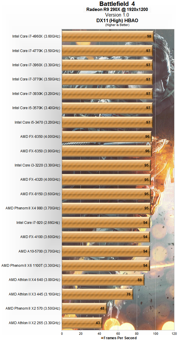
El 90 % de los juegos son gpu bound, es decir la grafica es la que limita el rendimiento, una grafica de gama alta como las que dices te darán un aumento de rendimiento brutal aunque tu cpu no las permita aprovechar al 100%, eso si overclockeado, a velocidad stock se te queda muy pequeña esa cpu, luego mas adelante cambia todo el ordenador y quédate con tu grafica.
una cpu gama alta + grafica gama media en el 90% de los casos dara menos rendimiento cpu gama baja + grafica gama alta.
como ejemplo bf4, fíjate la poca diferencia con cpu que cuestan 3 veces menos.
Mirando el CPU-Z veo que mi procesador es revision G0, asi k imagino k se le pueda dar un poco de chicha, pero no se si mi Asus Silent Knight podra disipar tanto calor.
En el tema de las memorias, no lo veo claro, os dejo el LOG del CPU-Z
Processors Information -------------------------------------------------------------------------
Processor 1 ID = 0 Number of cores 4 (max 4) Number of threads 4 (max 4) Name Intel Core 2 Quad Q6600 Codename Kentsfield Specification Intel(R) Core(TM)2 Quad CPU Q6600 @ 2.40GHz Package (platform ID) Socket 775 LGA (0x4) CPUID 6.F.B Extended CPUID 6.F Core Stepping G0 Technology 65 nm Core Speed 2399.8 MHz Multiplier x Bus Speed 9.0 x 266.6 MHz Rated Bus speed 1066.6 MHz Stock frequency 2400 MHz Instructions sets MMX, SSE, SSE2, SSE3, SSSE3, EM64T, VT-x L1 Data cache 4 x 32 KBytes, 8-way set associative, 64-byte line size L1 Instruction cache 4 x 32 KBytes, 8-way set associative, 64-byte line size L2 cache 2 x 4096 KBytes, 16-way set associative, 64-byte line size FID/VID Control yes FID range 6.0x - 9.0x Max VID 1.325 V
Hardware monitor ITE IT87 Voltage 0 1.25 Volts [0x4E] (CPU VCORE) Voltage 1 3.26 Volts [0xCC] (+3.3V) Voltage 3 5.05 Volts [0xBC] (+5V) Voltage 4 11.90 Volts [0xBA] (+12V) Voltage 7 4.92 Volts [0xB7] (+5V VCCH) Temperature 0 29°C (84°F) [0x1D] (CPU) Temperature 1 34°C (93°F) [0x22] (Mainboard) Fan 0 2411 RPM [0x118] (FANIN0) Fan PWM 0 99 pc [0x7F] (FANPWM0) Fan PWM 1 99 pc [0x7F] (FANPWM1) Fan PWM 2 0 pc [0x0] (FANPWM2) Register space LPC, base address = 0x0290
Hardware monitor Analog Device ADT7475 Voltage 1 3.29 Volts [0x2FC] (+3.3V) Temperature 1 36°C (96°F) [0x64] (Local) Fan PWM 0 100 pc [0xFF] (PWM1) Fan PWM 1 0 pc [0x0] (PWM2) Fan PWM 2 0 pc [0x0] (PWM3) Register space SMBus, base address = 0x01C80 SMBus request channel 0x0, address 0x2E
Hardware monitor Winbond W83791D Voltage 0 1.26 Volts [0x4F] (HT 1.2V) Voltage 1 1.54 Volts [0x60] (SB Core) Voltage 2 1.17 Volts [0x49] (CPU VTT) Voltage 4 2.14 Volts [0x43] (DDR) Voltage 6 1.25 Volts [0x4E] (NB Core) Register space SMBus, base address = 0x01C80 SMBus request channel 0x0, address 0x2D
Hardware monitor ACPI Temperature 0 40°C (104°F) [0xC3C] (THRM)
Hardware monitor NVIDIA NVAPI Voltage 0 1.05 Volts [0x41A] (VIN0) Temperature 0 51°C (123°F) [0x33] (TMPIN0) Fan PWM 0 40 pc [0x28] (FANPWMIN0)
Description Host Bridge Location bus 0 (0x00), device 0 (0x00), function 0 (0x00) Common header Vendor ID 0x10DE Model ID 0x03A1 Revision ID 0xA2 PI 0x00 SubClass 0x00 BaseClass 0x06 Cache Line 0x00 Latency 0x00 Header 0x80 PCI header Subvendor ID 0x0000 Subsystem ID 0x0000 Int. Line 0x00 Int. Pin 0x00 PCI capability Caps class HyperTransport Caps offset 0x40 Caps revision 0.16 Interface type Host/Secondary Device number 0 Link 0 width (in/out) 8 bits/8 bits Link 0 frequency 1000 MHz PCI registers
Description RAM Memory Controller Location bus 0 (0x00), device 0 (0x00), function 1 (0x01) Common header Vendor ID 0x10DE Model ID 0x03AC Revision ID 0xA1 PI 0x00 SubClass 0x00 BaseClass 0x05 Cache Line 0x00 Latency 0x00 Header 0x80 PCI header Subvendor ID 0x0000 Subsystem ID 0x0000 Int. Line 0x00 Int. Pin 0x00 PCI registers
Description RAM Memory Controller Location bus 0 (0x00), device 0 (0x00), function 2 (0x02) Common header Vendor ID 0x10DE Model ID 0x03AA Revision ID 0xA1 PI 0x00 SubClass 0x00 BaseClass 0x05 Cache Line 0x00 Latency 0x00 Header 0x80 PCI header Subvendor ID 0x0000 Subsystem ID 0x0000 Int. Line 0x00 Int. Pin 0x00 PCI registers
Description RAM Memory Controller Location bus 0 (0x00), device 0 (0x00), function 3 (0x03) Common header Vendor ID 0x10DE Model ID 0x03A9 Revision ID 0xA1 PI 0x00 SubClass 0x00 BaseClass 0x05 Cache Line 0x00 Latency 0x00 Header 0x00 PCI header Subvendor ID 0x0000 Subsystem ID 0x0000 Int. Line 0x00 Int. Pin 0x00 PCI registers
Description RAM Memory Controller Location bus 0 (0x00), device 0 (0x00), function 4 (0x04) Common header Vendor ID 0x10DE Model ID 0x03AB Revision ID 0xA1 PI 0x00 SubClass 0x00 BaseClass 0x05 Cache Line 0x00 Latency 0x00 Header 0x00 PCI header Subvendor ID 0x0000 Subsystem ID 0x0000 Int. Line 0x00 Int. Pin 0x00 PCI registers
Description RAM Memory Controller Location bus 0 (0x00), device 0 (0x00), function 5 (0x05) Common header Vendor ID 0x10DE Model ID 0x03A8 Revision ID 0xA2 PI 0x00 SubClass 0x00 BaseClass 0x05 Cache Line 0x00 Latency 0x00 Header 0x80 PCI header Subvendor ID 0x0000 Subsystem ID 0x0000 Int. Line 0x00 Int. Pin 0x00 PCI registers
Description RAM Memory Controller Location bus 0 (0x00), device 0 (0x00), function 6 (0x06) Common header Vendor ID 0x10DE Model ID 0x03B5 Revision ID 0xA1 PI 0x00 SubClass 0x00 BaseClass 0x05 Cache Line 0x00 Latency 0x00 Header 0x80 PCI header Subvendor ID 0x0000 Subsystem ID 0x0000 Int. Line 0x00 Int. Pin 0x00 PCI registers
Description RAM Memory Controller Location bus 0 (0x00), device 0 (0x00), function 7 (0x07) Common header Vendor ID 0x10DE Model ID 0x03B4 Revision ID 0xA1 PI 0x00 SubClass 0x00 BaseClass 0x05 Cache Line 0x00 Latency 0x00 Header 0x80 PCI header Subvendor ID 0x0000 Subsystem ID 0x0000 Int. Line 0x00 Int. Pin 0x00 PCI registers
Description RAM Memory Controller Location bus 0 (0x00), device 1 (0x01), function 0 (0x00) Common header Vendor ID 0x10DE Model ID 0x03AD Revision ID 0xA1 PI 0x00 SubClass 0x00 BaseClass 0x05 Cache Line 0x00 Latency 0x00 Header 0x80 PCI header Subvendor ID 0x0000 Subsystem ID 0x0000 Int. Line 0x00 Int. Pin 0x00 PCI registers
Description RAM Memory Controller Location bus 0 (0x00), device 1 (0x01), function 1 (0x01) Common header Vendor ID 0x10DE Model ID 0x03AE Revision ID 0xA1 PI 0x00 SubClass 0x00 BaseClass 0x05 Cache Line 0x00 Latency 0x00 Header 0x80 PCI header Subvendor ID 0x0000 Subsystem ID 0x0000 Int. Line 0x00 Int. Pin 0x00 PCI registers
Description RAM Memory Controller Location bus 0 (0x00), device 1 (0x01), function 2 (0x02) Common header Vendor ID 0x10DE Model ID 0x03AF Revision ID 0xA1 PI 0x00 SubClass 0x00 BaseClass 0x05 Cache Line 0x00 Latency 0x00 Header 0x80 PCI header Subvendor ID 0x0000 Subsystem ID 0x0000 Int. Line 0x00 Int. Pin 0x00 PCI registers
Description RAM Memory Controller Location bus 0 (0x00), device 1 (0x01), function 3 (0x03) Common header Vendor ID 0x10DE Model ID 0x03B0 Revision ID 0xA1 PI 0x00 SubClass 0x00 BaseClass 0x05 Cache Line 0x00 Latency 0x00 Header 0x80 PCI header Subvendor ID 0x0000 Subsystem ID 0x0000 Int. Line 0x00 Int. Pin 0x00 PCI registers
Description RAM Memory Controller Location bus 0 (0x00), device 1 (0x01), function 4 (0x04) Common header Vendor ID 0x10DE Model ID 0x03B1 Revision ID 0xA1 PI 0x00 SubClass 0x00 BaseClass 0x05 Cache Line 0x00 Latency 0x00 Header 0x80 PCI header Subvendor ID 0x0000 Subsystem ID 0x0000 Int. Line 0x00 Int. Pin 0x00 PCI registers
Description RAM Memory Controller Location bus 0 (0x00), device 1 (0x01), function 5 (0x05) Common header Vendor ID 0x10DE Model ID 0x03B2 Revision ID 0xA1 PI 0x00 SubClass 0x00 BaseClass 0x05 Cache Line 0x00 Latency 0x00 Header 0x80 PCI header Subvendor ID 0x0000 Subsystem ID 0x0000 Int. Line 0x00 Int. Pin 0x00 PCI registers
Description RAM Memory Controller Location bus 0 (0x00), device 1 (0x01), function 6 (0x06) Common header Vendor ID 0x10DE Model ID 0x03B3 Revision ID 0xA1 PI 0x00 SubClass 0x00 BaseClass 0x05 Cache Line 0x00 Latency 0x00 Header 0x80 PCI header Subvendor ID 0x0000 Subsystem ID 0x0000 Int. Line 0x00 Int. Pin 0x00 PCI registers
Description RAM Memory Controller Location bus 0 (0x00), device 2 (0x02), function 0 (0x00) Common header Vendor ID 0x10DE Model ID 0x03B6 Revision ID 0xA1 PI 0x00 SubClass 0x00 BaseClass 0x05 Cache Line 0x00 Latency 0x00 Header 0x80 PCI header Subvendor ID 0x0000 Subsystem ID 0x0000 Int. Line 0x00 Int. Pin 0x00 PCI registers
Description RAM Memory Controller Location bus 0 (0x00), device 2 (0x02), function 1 (0x01) Common header Vendor ID 0x10DE Model ID 0x03BC Revision ID 0xA1 PI 0x00 SubClass 0x00 BaseClass 0x05 Cache Line 0x00 Latency 0x00 Header 0x00 PCI header Subvendor ID 0x0000 Subsystem ID 0x0000 Int. Line 0x00 Int. Pin 0x00 PCI registers 00 01 02 03 04 05 06 07 08 09 0A 0B 0C 0D 0E 0F 00
Description RAM Memory Controller Location bus 0 (0x00), device 2 (0x02), function 2 (0x02) Common header Vendor ID 0x10DE Model ID 0x03BA Revision ID 0xA1 PI 0x00 SubClass 0x00 BaseClass 0x05 Cache Line 0x00 Latency 0x00 Header 0x80 PCI header Subvendor ID 0x0000 Subsystem ID 0x0000 Int. Line 0x00 Int. Pin 0x00 PCI registers
Description PCI to PCI Bridge Location bus 0 (0x00), device 3 (0x03), function 0 (0x00) Common header Vendor ID 0x10DE Model ID 0x03B7 Revision ID 0xA1 PI 0x00 SubClass 0x04 BaseClass 0x06 Cache Line 0x08 Latency 0x00 Header 0x01 PCI header Primary bus 0x00 Secondary bus 0x01 Int. Line 0x00 Int. Pin 0x00 PCI capability Caps class Subsystem Vendor Caps offset 0x40 SubVendor ID 0x10DE SubSystem ID 0x0C55 PCI capability Caps class Power Management Caps offset 0x48 Caps version 1.1 PCI capability Caps class Message Signalled Interrupts Caps offset 0x50 PCI capability Caps class HyperTransport Caps offset 0x60 Interface type MSI Mapping PCI capability Caps class PCI Express Caps offset 0x80 Device type Root Port of PCI-E Root Complex Port 0 Version 1.0 Physical slot #0 Presence detect yes Link width 16x (max 16x) Extended capabilities Caps class Virtual Channel Caps offset 0x100 PCI registers
Description RAM Memory Controller Location bus 0 (0x00), device 9 (0x09), function 0 (0x00) Common header Vendor ID 0x10DE Model ID 0x0369 Revision ID 0xA1 PI 0x00 SubClass 0x00 BaseClass 0x05 Cache Line 0x00 Latency 0x00 Header 0x00 PCI header Subvendor ID 0x1043 Subsystem ID 0xCB84 Int. Line 0x00 Int. Pin 0x00 PCI capability Caps class HyperTransport Caps offset 0x44 Caps revision 1.03 Interface type Slave/Primary Link 0 width (in/out) 8 bits/8 bits Link 0 frequency 1000 MHz Link 1 width (in/out) 8 bits/8 bits Link 1 frequency 200 MHz PCI capability Caps class 0x0 Caps offset 0xE0 PCI registers
Description PCI to ISA Bridge Location bus 0 (0x00), device 10 (0x0A), function 0 (0x00) Common header Vendor ID 0x10DE Model ID 0x0360 Revision ID 0xA2 PI 0x00 SubClass 0x01 BaseClass 0x06 Cache Line 0x00 Latency 0x00 Header 0x80 PCI header Subvendor ID 0x1043 Subsystem ID 0xCB84 Int. Line 0xFF Int. Pin 0x00 PCI registers
Description SMBus Controller Location bus 0 (0x00), device 10 (0x0A), function 1 (0x01) Common header Vendor ID 0x10DE Model ID 0x0368 Revision ID 0xA2 PI 0x00 SubClass 0x05 BaseClass 0x0C Cache Line 0x00 Latency 0x00 Header 0x80 PCI header Address 0 (port) 0x0000FF00 Address 4 (port) 0x00001C00 Address 5 (port) 0x00001C80 Subvendor ID 0x1043 Subsystem ID 0xCB84 Int. Line 0x05 Int. Pin 0x01 PCI capability Caps class Power Management Caps offset 0x44 Caps version 1.1 PCI registers
Description USB Controller (OHCI) Location bus 0 (0x00), device 11 (0x0B), function 0 (0x00) Common header Vendor ID 0x10DE Model ID 0x036C Revision ID 0xA1 PI 0x10 SubClass 0x03 BaseClass 0x0C Cache Line 0x00 Latency 0x00 Header 0x80 PCI header Address 0 (memory) 0xEFFFF000 Subvendor ID 0x1043 Subsystem ID 0xCB84 Int. Line 0x14 Int. Pin 0x01 PCI capability Caps class Power Management Caps offset 0x44 Caps version 1.1 PCI registers
Description USB 2.0 Controller (EHCI) Location bus 0 (0x00), device 11 (0x0B), function 1 (0x01) Common header Vendor ID 0x10DE Model ID 0x036D Revision ID 0xA2 PI 0x20 SubClass 0x03 BaseClass 0x0C Cache Line 0x00 Latency 0x00 Header 0x80 PCI header Address 0 (memory) 0xEFFFE000 Subvendor ID 0x1043 Subsystem ID 0xCB84 Int. Line 0x17 Int. Pin 0x02 PCI capability Caps class Debug Port Caps offset 0x44 PCI capability Caps class Power Management Caps offset 0x80 Caps version 1.1 PCI registers
Description IDE Controller Location bus 0 (0x00), device 13 (0x0D), function 0 (0x00) Common header Vendor ID 0x10DE Model ID 0x036E Revision ID 0xA1 PI 0x8A SubClass 0x01 BaseClass 0x01 Cache Line 0x00 Latency 0x00 Header 0x00 PCI header Address 4 (port) 0x0000FC00 Subvendor ID 0x1043 Subsystem ID 0xCB84 Int. Line 0x00 Int. Pin 0x00 PCI capability Caps class Power Management Caps offset 0x44 Caps version 1.1 PCI registers
Description IDE Controller Location bus 0 (0x00), device 14 (0x0E), function 0 (0x00) Common header Vendor ID 0x10DE Model ID 0x037F Revision ID 0xA2 PI 0x85 SubClass 0x01 BaseClass 0x01 Cache Line 0x00 Latency 0x00 Header 0x80 PCI header Address 0 (port) 0x000009F0 Address 1 (port) 0x00000BF0 Address 2 (port) 0x00000970 Address 3 (port) 0x00000B70 Address 4 (port) 0x0000F700 Address 5 (memory) 0xEFFFD000 Subvendor ID 0x1043 Subsystem ID 0xCB84 Int. Line 0x16 Int. Pin 0x01 PCI capability Caps class Power Management Caps offset 0x44 Caps version 1.1 PCI capability Caps class Message Signalled Interrupts Caps offset 0xB0 PCI capability Caps class HyperTransport Caps offset 0xCC Interface type MSI Mapping PCI registers
Description IDE Controller Location bus 0 (0x00), device 14 (0x0E), function 1 (0x01) Common header Vendor ID 0x10DE Model ID 0x037F Revision ID 0xA2 PI 0x85 SubClass 0x01 BaseClass 0x01 Cache Line 0x00 Latency 0x00 Header 0x80 PCI header Address 0 (port) 0x000009E0 Address 1 (port) 0x00000BE0 Address 2 (port) 0x00000960 Address 3 (port) 0x00000B60 Address 4 (port) 0x0000F200 Address 5 (memory) 0xEFFFC000 Subvendor ID 0x1043 Subsystem ID 0xCB84 Int. Line 0x17 Int. Pin 0x02 PCI capability Caps class Power Management Caps offset 0x44 Caps version 1.1 PCI capability Caps class Message Signalled Interrupts Caps offset 0xB0 PCI capability Caps class HyperTransport Caps offset 0xCC Interface type MSI Mapping PCI registers
Description RAID Controller Location bus 0 (0x00), device 14 (0x0E), function 2 (0x02) Common header Vendor ID 0x10DE Model ID 0x037F Revision ID 0xA2 PI 0x85 SubClass 0x04 BaseClass 0x01 Cache Line 0x00 Latency 0x00 Header 0x80 PCI header Address 0 (port) 0x0000F100 Address 1 (port) 0x0000F000 Address 2 (port) 0x0000EF00 Address 3 (port) 0x0000EE00 Address 4 (port) 0x0000ED00 Address 5 (memory) 0xEFFFB000 Subvendor ID 0x1043 Subsystem ID 0xCB84 Int. Line 0x14 Int. Pin 0x03 PCI capability Caps class Power Management Caps offset 0x44 Caps version 1.1 PCI capability Caps class Message Signalled Interrupts Caps offset 0xB0 PCI capability Caps class HyperTransport Caps offset 0xCC Interface type MSI Mapping PCI registers
Description PCI to PCI Bridge Location bus 0 (0x00), device 15 (0x0F), function 0 (0x00) Common header Vendor ID 0x10DE Model ID 0x0370 Revision ID 0xA2 PI 0x01 SubClass 0x04 BaseClass 0x06 Cache Line 0x00 Latency 0x00 Header 0x81 PCI header Primary bus 0x00 Secondary bus 0x02 Int. Line 0xFF Int. Pin 0x00 PCI capability Caps class Subsystem Vendor Caps offset 0xB8 SubVendor ID 0x10DE SubSystem ID 0xCB84 PCI capability Caps class HyperTransport Caps offset 0x8C Interface type MSI Mapping PCI registers
Description Multimedia device Location bus 0 (0x00), device 15 (0x0F), function 1 (0x01) Common header Vendor ID 0x10DE Model ID 0x0371 Revision ID 0xA2 PI 0x00 SubClass 0x03 BaseClass 0x04 Cache Line 0x00 Latency 0x00 Header 0x80 PCI header Address 0 (memory) 0xEFFF0000 Subvendor ID 0x1043 Subsystem ID 0x81F2 Int. Line 0x15 Int. Pin 0x02 PCI capability Caps class Power Management Caps offset 0x44 Caps version 1.1 PCI capability Caps class Message Signalled Interrupts Caps offset 0x50 PCI capability Caps class HyperTransport Caps offset 0x6C Interface type MSI Mapping PCI registers
Description Bridge device Location bus 0 (0x00), device 17 (0x11), function 0 (0x00) Common header Vendor ID 0x10DE Model ID 0x0373 Revision ID 0xA2 PI 0x00 SubClass 0x80 BaseClass 0x06 Cache Line 0x00 Latency 0x00 Header 0x00 PCI header Address 0 (memory) 0xEFFFA000 Address 2 (memory) 0xEFFF9000 Address 3 (memory) 0xEFFF8000 Subvendor ID 0x1043 Subsystem ID 0xCB84 Int. Line 0x14 Int. Pin 0x01 PCI capability Caps class Power Management Caps offset 0x44 Caps version 1.1 PCI capability Caps class MSI-X Caps offset 0x70 PCI capability Caps class Message Signalled Interrupts Caps offset 0x50 PCI capability Caps class HyperTransport Caps offset 0x6C Interface type MSI Mapping PCI registers
Description Bridge device Location bus 0 (0x00), device 18 (0x12), function 0 (0x00) Common header Vendor ID 0x10DE Model ID 0x0373 Revision ID 0xA2 PI 0x00 SubClass 0x80 BaseClass 0x06 Cache Line 0x00 Latency 0x00 Header 0x00 PCI header Address 0 (memory) 0xEFFF7000 Address 2 (memory) 0xEFFF6000 Address 3 (memory) 0xEFFF5000 Subvendor ID 0x1043 Subsystem ID 0xCB84 Int. Line 0x17 Int. Pin 0x01 PCI capability Caps class Power Management Caps offset 0x44 Caps version 1.1 PCI capability Caps class MSI-X Caps offset 0x70 PCI capability Caps class Message Signalled Interrupts Caps offset 0x50 PCI capability Caps class HyperTransport Caps offset 0x6C Interface type MSI Mapping PCI registers
Description PCI to PCI Bridge Location bus 0 (0x00), device 19 (0x13), function 0 (0x00) Common header Vendor ID 0x10DE Model ID 0x0376 Revision ID 0xA2 PI 0x00 SubClass 0x04 BaseClass 0x06 Cache Line 0x08 Latency 0x00 Header 0x01 PCI header Primary bus 0x00 Secondary bus 0x03 Int. Line 0x00 Int. Pin 0x00 PCI capability Caps class Subsystem Vendor Caps offset 0x40 SubVendor ID 0x10DE SubSystem ID 0x0000 PCI capability Caps class Power Management Caps offset 0x48 Caps version 1.1 PCI capability Caps class Message Signalled Interrupts Caps offset 0x50 PCI capability Caps class HyperTransport Caps offset 0x60 Interface type MSI Mapping PCI capability Caps class PCI Express Caps offset 0x80 Device type Root Port of PCI-E Root Complex Port 5 Version 1.0 Physical slot #0 Presence detect no Link width 8x (max 8x) Extended capabilities Caps class Virtual Channel Caps offset 0x100 PCI registers
Description PCI to PCI Bridge Location bus 0 (0x00), device 22 (0x16), function 0 (0x00) Common header Vendor ID 0x10DE Model ID 0x0378 Revision ID 0xA2 PI 0x00 SubClass 0x04 BaseClass 0x06 Cache Line 0x08 Latency 0x00 Header 0x01 PCI header Primary bus 0x00 Secondary bus 0x04 Int. Line 0x00 Int. Pin 0x00 PCI capability Caps class Subsystem Vendor Caps offset 0x40 SubVendor ID 0x10DE SubSystem ID 0x0000 PCI capability Caps class Power Management Caps offset 0x48 Caps version 1.1 PCI capability Caps class Message Signalled Interrupts Caps offset 0x50 PCI capability Caps class HyperTransport Caps offset 0x60 Interface type MSI Mapping PCI capability Caps class PCI Express Caps offset 0x80 Device type Root Port of PCI-E Root Complex Port 2 Version 1.0 Physical slot #0 Presence detect yes Link width 1x (max 1x) Extended capabilities Caps class Virtual Channel Caps offset 0x100 PCI registers
Description PCI to PCI Bridge Location bus 0 (0x00), device 24 (0x18), function 0 (0x00) Common header Vendor ID 0x10DE Model ID 0x0377 Revision ID 0xA2 PI 0x00 SubClass 0x04 BaseClass 0x06 Cache Line 0x08 Latency 0x00 Header 0x01 PCI header Primary bus 0x00 Secondary bus 0x05 Int. Line 0x00 Int. Pin 0x00 PCI capability Caps class Subsystem Vendor Caps offset 0x40 SubVendor ID 0x10DE SubSystem ID 0x0000 PCI capability Caps class Power Management Caps offset 0x48 Caps version 1.1 PCI capability Caps class Message Signalled Interrupts Caps offset 0x50 PCI capability Caps class HyperTransport Caps offset 0x60 Interface type MSI Mapping PCI capability Caps class PCI Express Caps offset 0x80 Device type Root Port of PCI-E Root Complex Port 0 Version 1.0 Physical slot #0 Presence detect yes Link width 4x (max 16x) Extended capabilities Caps class Virtual Channel Caps offset 0x100 PCI registers
Description VGA Controller Location bus 1 (0x01), device 0 (0x00), function 0 (0x00) Common header Vendor ID 0x10DE Model ID 0x05E6 Revision ID 0xA1 PI 0x00 SubClass 0x00 BaseClass 0x03 Cache Line 0x08 Latency 0x00 Header 0x00 PCI header Address 0 (memory) 0xE8000000 Address 1 (memory) 0xD0000000 Address 3 (memory) 0xE6000000 Address 5 (port) 0x0000DC00 Subvendor ID 0x1458 Subsystem ID 0x34CE Int. Line 0x10 Int. Pin 0x01 PCI capability Caps class Power Management Caps offset 0x60 Caps version 1.2 PCI capability Caps class Message Signalled Interrupts Caps offset 0x68 PCI capability Caps class PCI Express Caps offset 0x78 Device type PCI-E Endpoint Device Port 0 Version 2.0 Link width 16x (max 16x) Extended capabilities Caps class Virtual Channel Caps offset 0x100 Caps class Power Budgeting Caps offset 0x128 Caps class Vendor Specific Caps offset 0x600 Vendor ID 1 Size 36 PCI registers
Location bus 2 (0x02), device 6 (0x06), function 0 (0x00) Common header Vendor ID 0x14F1 Model ID 0x8800 Revision ID 0x05 PI 0x00 SubClass 0x00 BaseClass 0x04 Cache Line 0x08 Latency 0x20 Header 0x80 PCI header Address 0 (memory) 0xEA000000 Subvendor ID 0x0070 Subsystem ID 0x6902 Int. Line 0x05 Int. Pin 0x01 PCI capability Caps class Virtual Product Data Caps offset 0x44 PCI capability Caps class Power Management Caps offset 0x4C Caps version 1.1 PCI registers
Description Multimedia device Location bus 2 (0x02), device 6 (0x06), function 1 (0x01) Common header Vendor ID 0x14F1 Model ID 0x8811 Revision ID 0x05 PI 0x00 SubClass 0x80 BaseClass 0x04 Cache Line 0x00 Latency 0x00 Header 0x80 PCI header Subvendor ID 0x0070 Subsystem ID 0x6902 Int. Line 0x00 Int. Pin 0x01 PCI capability Caps class Power Management Caps offset 0x4C Caps version 1.1 PCI registers
Description Multimedia device Location bus 2 (0x02), device 6 (0x06), function 2 (0x02) Common header Vendor ID 0x14F1 Model ID 0x8802 Revision ID 0x05 PI 0x00 SubClass 0x80 BaseClass 0x04 Cache Line 0x00 Latency 0x00 Header 0x80 PCI header Subvendor ID 0x0070 Subsystem ID 0x6902 Int. Line 0x00 Int. Pin 0x01 PCI capability Caps class Power Management Caps offset 0x4C Caps version 1.1 PCI registers
Description Multimedia device Location bus 2 (0x02), device 6 (0x06), function 4 (0x04) Common header Vendor ID 0x14F1 Model ID 0x8804 Revision ID 0x05 PI 0x00 SubClass 0x80 BaseClass 0x04 Cache Line 0x00 Latency 0x00 Header 0x80 PCI header Subvendor ID 0x0070 Subsystem ID 0x6902 Int. Line 0x00 Int. Pin 0x01 PCI capability Caps class Power Management Caps offset 0x4C Caps version 1.1 PCI registers
Description OHCI FireWire Controller Location bus 2 (0x02), device 11 (0x0B), function 0 (0x00) Common header Vendor ID 0x1106 Model ID 0x3044 Revision ID 0xC0 PI 0x10 SubClass 0x00 BaseClass 0x0C Cache Line 0x08 Latency 0x20 Header 0x00 PCI header Address 0 (memory) 0xEEFFF000 Address 1 (port) 0x0000CC00 Subvendor ID 0x1043 Subsystem ID 0x81FE Int. Line 0x13 Int. Pin 0x01 PCI capability Caps class Power Management Caps offset 0x50 Caps version 1.1 PCI registers
Description Mass storage Controller Location bus 4 (0x04), device 0 (0x00), function 0 (0x00) Common header Vendor ID 0x1095 Model ID 0x3132 Revision ID 0x01 PI 0x00 SubClass 0x80 BaseClass 0x01 Cache Line 0x08 Latency 0x00 Header 0x00 PCI header Address 0 (memory) 0xEFBFF000 Address 2 (memory) 0xEFBF8000 Address 4 (port) 0x0000AC00 Subvendor ID 0x1043 Subsystem ID 0x819F Int. Line 0x0B Int. Pin 0x01 PCI capability Caps class Power Management Caps offset 0x54 Caps version 1.1 PCI capability Caps class Message Signalled Interrupts Caps offset 0x5C PCI capability Caps class PCI Express Caps offset 0x70 Device type Legacy PCI-E Endpoint Device Port 0 Version 1.0 Link width 1x (max 1x) Extended capabilities Caps class Advanced Error Reporting Caps offset 0x100 PCI registers
Description PCI to PCI Bridge Location bus 5 (0x05), device 0 (0x00), function 0 (0x00) Common header Vendor ID 0x10B5 Model ID 0x8608 Revision ID 0xBA PI 0x00 SubClass 0x04 BaseClass 0x06 Cache Line 0x08 Latency 0x00 Header 0x01 PCI header Address 0 (memory) 0xEF9E0000 Primary bus 0x05 Secondary bus 0x06 Int. Line 0x10 Int. Pin 0x01 PCI capability Caps class Power Management Caps offset 0x40 Caps version 1.2 PCI capability Caps class Message Signalled Interrupts Caps offset 0x48 PCI capability Caps class PCI Express Caps offset 0x68 Device type Upstream Port of PCI-E Switch Port 0 Version 2.0 Link width 4x (max 4x) PCI capability Caps class Subsystem Vendor Caps offset 0xA4 SubVendor ID 0x10B5 SubSystem ID 0x8608 Extended capabilities Caps class Device Serial Number Caps offset 0x100 Caps class Advanced Error Reporting Caps offset 0xFB4 Caps class Power Budgeting Caps offset 0x138 Caps class Virtual Channel Caps offset 0x148 Caps class Vendor Specific Caps offset 0x448 Vendor ID 0 Size 204 Caps class Vendor Specific Caps offset 0x950 Vendor ID 1 Size 16 PCI registers
Description PCI to PCI Bridge Location bus 6 (0x06), device 1 (0x01), function 0 (0x00) Common header Vendor ID 0x10B5 Model ID 0x8608 Revision ID 0xBA PI 0x00 SubClass 0x04 BaseClass 0x06 Cache Line 0x08 Latency 0x00 Header 0x01 PCI header Primary bus 0x06 Secondary bus 0x07 Int. Line 0x10 Int. Pin 0x01 PCI capability Caps class Power Management Caps offset 0x40 Caps version 1.2 PCI capability Caps class Message Signalled Interrupts Caps offset 0x48 PCI capability Caps class PCI Express Caps offset 0x68 Device type Downstream Port of PCI-E Switch Port 1 Version 2.0 Physical slot #14 Presence detect yes Link width 1x (max 1x) PCI capability Caps class Subsystem Vendor Caps offset 0xA4 SubVendor ID 0x10B5 SubSystem ID 0x8608 Extended capabilities Caps class Device Serial Number Caps offset 0x100 Caps class Advanced Error Reporting Caps offset 0xFB4 Caps class Virtual Channel Caps offset 0x148 Caps class 0xD Caps offset 0x520 Caps class Vendor Specific Caps offset 0x950 Vendor ID 1 Size 16 PCI registers
Description PCI to PCI Bridge Location bus 6 (0x06), device 5 (0x05), function 0 (0x00) Common header Vendor ID 0x10B5 Model ID 0x8608 Revision ID 0xBA PI 0x00 SubClass 0x04 BaseClass 0x06 Cache Line 0x08 Latency 0x00 Header 0x01 PCI header Primary bus 0x06 Secondary bus 0x08 Int. Line 0x10 Int. Pin 0x01 PCI capability Caps class Power Management Caps offset 0x40 Caps version 1.2 PCI capability Caps class Message Signalled Interrupts Caps offset 0x48 PCI capability Caps class PCI Express Caps offset 0x68 Device type Downstream Port of PCI-E Switch Port 5 Version 2.0 Physical slot #14 Presence detect yes Link width 1x (max 1x) PCI capability Caps class Subsystem Vendor Caps offset 0xA4 SubVendor ID 0x10B5 SubSystem ID 0x8608 Extended capabilities Caps class Device Serial Number Caps offset 0x100 Caps class Advanced Error Reporting Caps offset 0xFB4 Caps class Virtual Channel Caps offset 0x148 Caps class 0xD Caps offset 0x520 Caps class Vendor Specific Caps offset 0x950 Vendor ID 1 Size 16 PCI registers
Description PCI to PCI Bridge Location bus 6 (0x06), device 7 (0x07), function 0 (0x00) Common header Vendor ID 0x10B5 Model ID 0x8608 Revision ID 0xBA PI 0x00 SubClass 0x04 BaseClass 0x06 Cache Line 0x08 Latency 0x00 Header 0x01 PCI header Primary bus 0x06 Secondary bus 0x09 Int. Line 0x10 Int. Pin 0x01 PCI capability Caps class Power Management Caps offset 0x40 Caps version 1.2 PCI capability Caps class Message Signalled Interrupts Caps offset 0x48 PCI capability Caps class PCI Express Caps offset 0x68 Device type Downstream Port of PCI-E Switch Port 7 Version 2.0 Physical slot #14 Presence detect no Link width 0x (max 1x) PCI capability Caps class Subsystem Vendor Caps offset 0xA4 SubVendor ID 0x10B5 SubSystem ID 0x8608 Extended capabilities Caps class Device Serial Number Caps offset 0x100 Caps class Advanced Error Reporting Caps offset 0xFB4 Caps class Virtual Channel Caps offset 0x148 Caps class 0xD Caps offset 0x520 Caps class Vendor Specific Caps offset 0x950 Vendor ID 1 Size 16 PCI registers
Description PCI to PCI Bridge Location bus 6 (0x06), device 9 (0x09), function 0 (0x00) Common header Vendor ID 0x10B5 Model ID 0x8608 Revision ID 0xBA PI 0x00 SubClass 0x04 BaseClass 0x06 Cache Line 0x08 Latency 0x00 Header 0x01 PCI header Primary bus 0x06 Secondary bus 0x0A Int. Line 0x10 Int. Pin 0x01 PCI capability Caps class Power Management Caps offset 0x40 Caps version 1.2 PCI capability Caps class Message Signalled Interrupts Caps offset 0x48 PCI capability Caps class PCI Express Caps offset 0x68 Device type Downstream Port of PCI-E Switch Port 9 Version 2.0 Physical slot #15 Presence detect no Link width 0x (max 1x) PCI capability Caps class Subsystem Vendor Caps offset 0xA4 SubVendor ID 0x10B5 SubSystem ID 0x8608 Extended capabilities Caps class Device Serial Number Caps offset 0x100 Caps class Advanced Error Reporting Caps offset 0xFB4 Caps class Virtual Channel Caps offset 0x148 Caps class 0xD Caps offset 0x520 Caps class Vendor Specific Caps offset 0x950 Vendor ID 1 Size 16 PCI registers
Description USB Controller Location bus 7 (0x07), device 0 (0x00), function 0 (0x00) Common header Vendor ID 0x1033 Model ID 0x0194 Revision ID 0x03 PI 0x30 SubClass 0x03 BaseClass 0x0C Cache Line 0x08 Latency 0x00 Header 0x00 PCI header Address 0 (memory) 0xEF8FE000 Subvendor ID 0x1043 Subsystem ID 0x8413 Int. Line 0x00 Int. Pin 0x01 PCI capability Caps class Power Management Caps offset 0x50 Caps version 1.2 PCI capability Caps class Message Signalled Interrupts Caps offset 0x70 PCI capability Caps class MSI-X Caps offset 0x90 PCI capability Caps class PCI Express Caps offset 0xA0 Device type PCI-E Endpoint Device Port 0 Version 2.0 Link width 1x (max 1x) Extended capabilities Caps class Advanced Error Reporting Caps offset 0x100 Caps class Device Serial Number Caps offset 0x140 Caps class 0x18 Caps offset 0x150 PCI registers
Description Serial ATA Controller Location bus 8 (0x08), device 0 (0x00), function 0 (0x00) Common header Vendor ID 0x1B4B Model ID 0x9120 Revision ID 0x12 PI 0x01 SubClass 0x06 BaseClass 0x01 Cache Line 0x08 Latency 0x00 Header 0x00 PCI header Address 0 (port) 0x00008C00 Address 1 (port) 0x00008800 Address 2 (port) 0x00008400 Address 3 (port) 0x00008000 Address 4 (port) 0x00007C00 Address 5 (memory) 0xEF7FF000 Subvendor ID 0x1043 Subsystem ID 0x8400 Int. Line 0x10 Int. Pin 0x01 PCI capability Caps class Power Management Caps offset 0x40 Caps version 1.2 PCI capability Caps class Message Signalled Interrupts Caps offset 0x50 PCI capability Caps class PCI Express Caps offset 0x70 Device type Legacy PCI-E Endpoint Device Port 0 Version 2.0 Link width 1x (max 1x) Extended capabilities Caps class Advanced Error Reporting Caps offset 0x100 PCI registers
DMI BIOS vendor Phoenix Technologies LTD version ASUS StrikerExtreme ACPI BIOS Revision 1901 date 04/28/2009 ROM size 1024 KB
DMI System Information manufacturer System manufacturer product System Product Name version System Version serial System Serial Number UUID {4A9377AC-9955-11DB-BD84-964393B234AB} SKU unknown family unknown
DMI Baseboard vendor ASUSTeK Computer INC. model StrikerExtreme revision 1.XX serial 123456789000
DMI System Enclosure manufacturer Chassis Manufacture chassis type Desktop chassis serial EVAL
DMI Port Connector designation PRI_IDE (internal) connector On Board IDE
DMI Port Connector designation FLOPPY (internal) port type 8251 FIFO Compatible connector On Board Floppy
DMI Port Connector designation PS/2 Keyboard (internal) port type Keyboard Port connector PS/2 connector PS/2
DMI Port Connector designation PS/2 Mouse (internal) port type Mouse Port connector PS/2 connector PS/2
DMI Port Connector designation USB1 (external) port type USB
DMI Port Connector designation USB2 (external) port type USB
DMI Port Connector designation USB3 (external) port type USB
DMI Port Connector designation USB4 (external) port type USB
DMI Port Connector designation USB5 (external) port type USB
DMI Port Connector designation USB6 (external) port type USB
DMI Port Connector designation USB7 (external) port type USB
DMI Port Connector designation USB8 (external) port type USB
DMI Port Connector designation USB9 (external) port type USB
DMI Port Connector designation USB10 (external) port type USB
DMI Port Connector designation LINE_IN (internal) designation LINE_IN (external) port type Audio Port
DMI Port Connector designation Back Surround L/R (internal) designation Back Surround L/R (external) port type Audio Port connector Mini Jack (headphones)
DMI Port Connector designation Side Surround L/R (internal) designation Side Surround L/R (external) port type Audio Port connector Mini Jack (headphones)
DMI Port Connector designation Center/LFE (internal) designation Center/LFE (external) port type Audio Port connector Mini Jack (headphones)
DMI Port Connector designation CD_IN (internal) designation CD_IN (external) port type Audio Port connector On Board Sound Input From CD-ROM
DMI Port Connector designation SPDIF_01 (external)
DMI Port Connector designation SPDIF_02 (external)
DMI Port Connector designation LAN_1 (external) port type Network Port connector RJ-45
DMI Port Connector designation LAN_2 (external) port type Network Port connector RJ-45
DMI Port Connector designation IE1394_1 (external) port type Firewire (IEEE P1394) connector IEEE 1394
DMI Port Connector designation IE1394_2 (external) port type Firewire (IEEE P1394) connector IEEE 1394
DMI Port Connector designation SATA1 (internal) connector On Board IDE
DMI Port Connector designation SATA2 (internal) connector On Board IDE
DMI Port Connector designation SATA3 (internal) connector On Board IDE
DMI Port Connector designation SATA4 (internal) connector On Board IDE
DMI Port Connector designation SATA5 (internal) connector On Board IDE
DMI Port Connector designation SATA6 (internal) connector On Board IDE
DMI Port Connector designation EX_SATA1 (internal) connector On Board IDE
DMI Port Connector designation EX_SATA2 (internal) connector On Board IDE
DMI Port Connector designation CHASSIS (internal)
DMI Port Connector designation ADH (internal)
DMI Port Connector designation AUDIO1 (internal)
DMI Port Connector designation CPU_FAN1 (internal)
DMI Port Connector designation OPT_FAN1 (internal)
DMI Port Connector designation OPT_FAN2 (internal)
DMI Port Connector designation OPT_FAN3 (internal)
DMI Port Connector designation OPT_FAN4 (internal)
DMI Port Connector designation OPT_FAN5 (internal)
DMI Port Connector designation PWR_FAN1 (internal)
DMI Port Connector designation CHA_FAN1 (internal)
Drive 0 Device Path \\?\scsi#disk&ven_corsair&prod_neutron_ssd&rev_m206#7&c9ffb&0&000100#{53f56307-b6bf-11d0-94f2-00a0c91efb8b} Type Fixed Name Corsair Neutron SSD Capacity 116.4 GB SMART Support Yes
Drive 1 Device Path \\?\scsi#disk&ven_st350063&prod_0as#4&1759b9db&0&000000#{53f56307-b6bf-11d0-94f2-00a0c91efb8b} Type Fixed Name ST350063 0AS Capacity 465.8 GB SMART Support Yes
Drive 2 Device Path \\?\scsi#disk____nvidia__stripe___223.58g#1#{53f56307-b6bf-11d0-94f2-00a0c91efb8b} Type Fixed Name NVIDIA STRIPE 223.58G Capacity 223.6 GB SMART Support Yes
Drive 3 Device Path \\?\usbstor#disk&ven_generic&prod_usb_cf_reader&rev_1.01#058f312d81b&1#{53f56307-b6bf-11d0-94f2-00a0c91efb8b} Type Fixed Name Generic USB CF Reader SMART Support Yes
Drive 4 Device Path \\?\usbstor#disk&ven_generic&prod_usb_ms_reader&rev_1.03#058f312d81b&3#{53f56307-b6bf-11d0-94f2-00a0c91efb8b} Type Fixed Name Generic USB MS Reader SMART Support Yes
Drive 5 Device Path \\?\usbstor#disk&ven_generic&prod_usb_sd_reader&rev_1.00#058f312d81b&0#{53f56307-b6bf-11d0-94f2-00a0c91efb8b} Type Fixed Name Generic USB SD Reader SMART Support Yes
Drive 6 Device Path \\?\usbstor#disk&ven_generic&prod_usb_sm_reader&rev_1.02#058f312d81b&2#{53f56307-b6bf-11d0-94f2-00a0c91efb8b} Type Fixed Name Generic USB SM Reader SMART Support Yes
USB Devices -------------------------------------------------------------------------
USB Device Dispositivo compuesto USB, class=0x00, subclass=0x00, vendor=0x046D, product=0xC512 USB Device Logitech USB Camera (Communicate STX), class=0x00, subclass=0x00, vendor=0x046D, product=0x08AD USB Device Dispositivo de almacenamiento USB, class=0x00, subclass=0x00, vendor=0x058F, product=0x6362 USB Device Dispositivo compuesto USB, class=0x00, subclass=0x00, vendor=0x046D, product=0x0A15
Windows Version Microsoft Windows 7 (6.1) 64-bit Service Pack 1 (Build 7601) DirectX Version 11.0
Mirando las tablas que ha puesto ismarub y elcaras veo que mi procesador ni se acerca al mas pequeño, tan mal me va ir? Cuanto seria lo máximo de procesador que le podria meter a esta placa de socket 775?
No puedo permitirme un pc nuevo, pero si una "pequeña" actualizacion, asi k si me decanto por la nvidia, que marca me recomendais? Asus, EVGA, MSI, Gygabyte??